發表文章

目前顯示的是 4月, 2018的文章

STM32F103 "Hello World" Part3

圖片
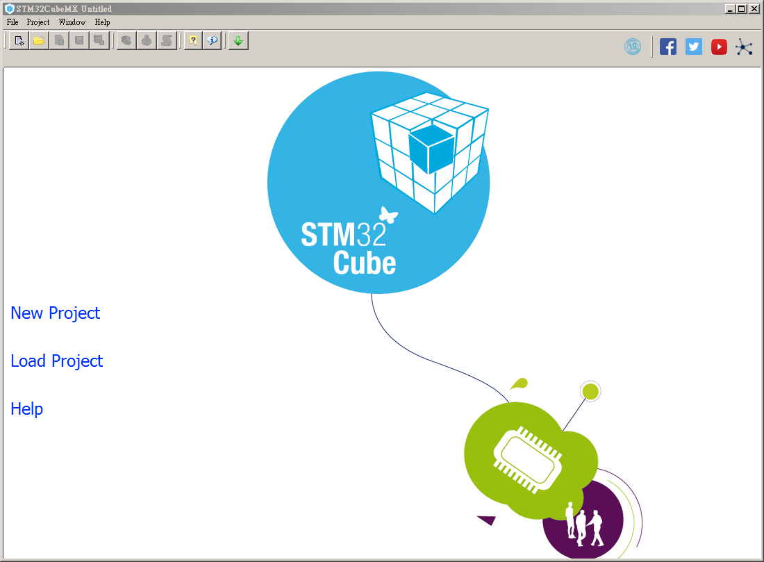
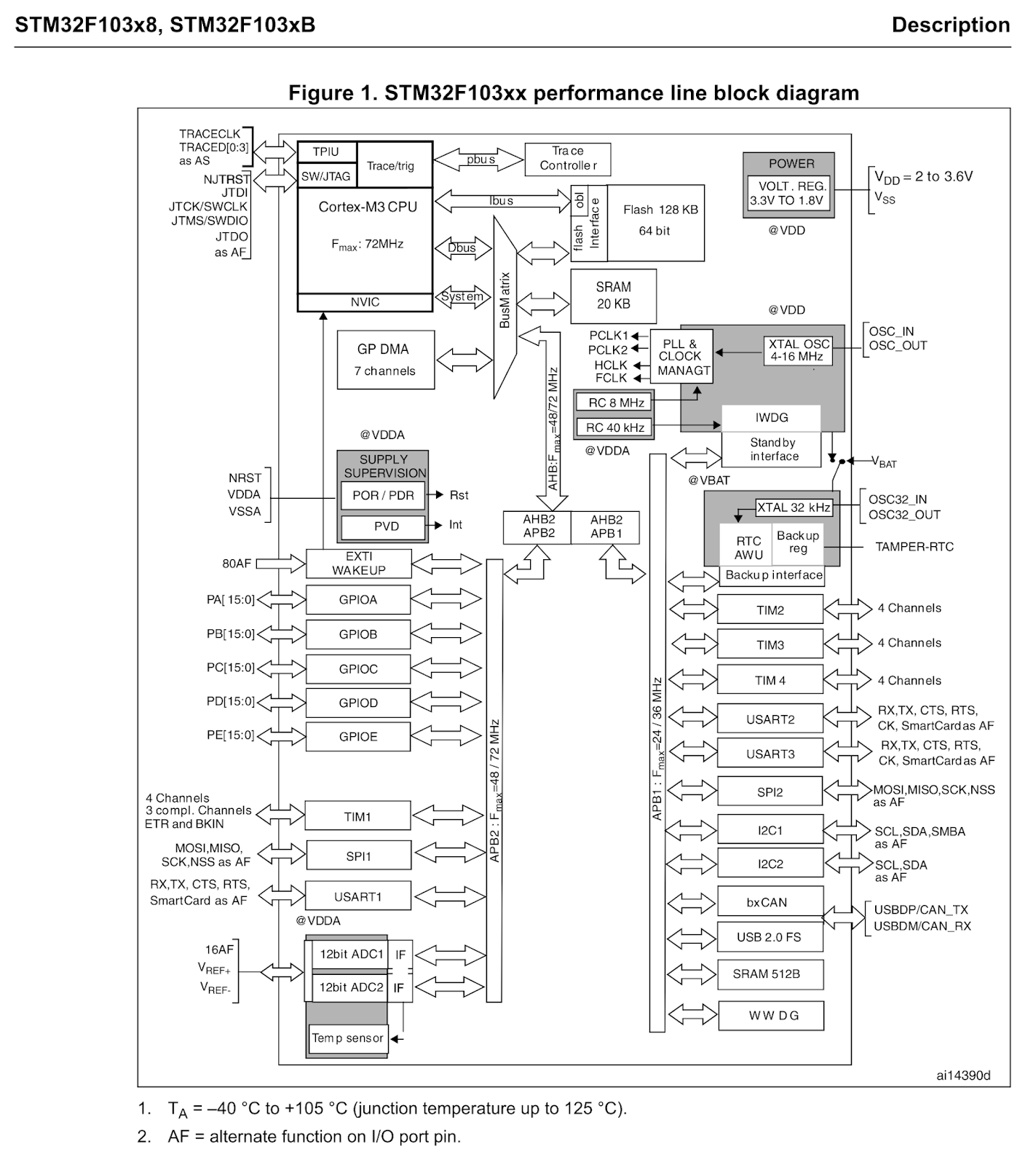
Purpose 本篇實際操作STM32CubeMX去生成initialization code Development board在Part1介紹 預計demo功能為USART, GPIO, HSE USART dump "Hello World", GPIO toggle LED, 使用Oscillator -> PLL -> 72MHz, 為system clock STM32CubeMX Version 4.25 Pin assignment USART1 : RX(PA_10), TX(PA_9) LED : PC_13 External Oscillator : OSC_IN(PD_0) & OSC_OUT(PD_1) 2-Wire Serial Debug : SWDIO(PA_13) & SWCLK(PA_14) Step by step Step 1. click New Project Step 2. 選擇MCU型號, 可透過下方Filter Search挑選MCU, 或直接 Part Number Search 輸入型號, 找到後連點兩次進去主畫面 Step 3. 主畫面 在Pinout分頁中可設定開啟或關閉各項Peripherals, 右邊為Chip View, 檢查Pin使用情況 Step 4. 設定各Peripherals, 如下圖左 RCC config 選擇 High Speed Clock (HSE) 為 Crystal/Ceramic Resonator SYS config 選擇 Debug 為 Serial Wire USART1 config 選擇 Mode 為 Asynchronous GPIO config 於Chip View選擇 PC13 為 GPIO Output 設定好後, 右邊Chip View顯示相對應的Pin assignment 被設定過的Peripherals與Pin會以不同顏色表示 於官方TRM (UM1718)有詳細定義, 下方列出常見define Step 5. 切換至 Clock Configuration

STM32F103 "Hello World" Part2

圖片
Block Diagram STM32F103xx series 內部為Cortex-M3 32-bit RISC架構, 最快系統時脈72MHz,  Ibus (Instruction Bus)為ARM core從Internal Flash提取指令bus,  Flash放置code與自定義資料etc. Dbus (Data Bus)為ARM core存取Internal SRAM的bus, SRAM內存放register variable System bus為MCU周邊控制器存取通道  Bus Matrix為調度ARM core與周邊的管理 AHB, APB為AMBA規範下的protocol, 常見於SoC, AMBA為通用協定, 提供core與peripherals間的bus AMBA(Advanced Micro-controller Bus Architecture) AHB(Advanced High performance Bus) APB(Advanced Peripheral Bus) STM32F103xx series AHB Fmax = 72MHz, APB2 Fmax = 72MHz, APB1 Fmax = 36MHz, 使用上需注意peripherals放置在哪一bus上, 影響到該peripherals Fmax Clock Tree SYSCLK source: HSI RC (8MHz) HSE PLL (MUL x2-16) *when the HSI is used as a PLL clock input, the maximum system clock frequency that can be achieved is 64MHz. *for the USB function to be available, both HSE and PLL must be enable, with USBCLK running at 48MHz. *to have an ADC conv. time of 1us, APB2 must be at 14MHz, 28MHz or 56MHz. RTC source: LSI (40kHz) LS